
materials are used in a PCB prototype
Creating a PCB prototype involves selecting materials that ensure the circuit board functions properly, remains durable, and can be manufactured efficiently. The choice of materials directly impacts the performance, cost, and manufacturability of the PCB. Understanding the different materials used in the creation of a PCB prototype is essential for engineers and designers to achieve the desired outcomes. In this article, we will explore the main materials commonly used in PCB prototypes and their roles in the design and production process.
The most common material used for the substrate in a PCB prototype is FR4 (Flame Retardant 4). FR4 is a type of fiberglass-reinforced epoxy laminate, widely chosen for its strong mechanical properties, excellent electrical insulation, and resistance to heat. FR4 offers a good balance of performance and cost, making it the material of choice for many general-purpose pcb prototype. Its availability and reliability in various applications, from consumer electronics to industrial systems, have made it the standard in PCB manufacturing.
Another material commonly used in PCB prototypes is CEM-1 (Composite Epoxy Material 1). CEM-1 is similar to FR4 but is composed of a paper-based material impregnated with epoxy resin. It is a more cost-effective option than FR4, though it may not offer the same level of durability or heat resistance. CEM-1 is often used in lower-cost, simple designs where high mechanical strength is not as critical. For PCB prototypes that do not require high performance or that are designed for short runs, CEM-1 can be a good alternative to FR4.
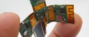
What materials are used in a PCB prototype?
For higher-performance PCB prototypes, especially those that need to withstand higher temperatures or offer better electrical performance, materials such as polyimide or PTFE (Teflon) are often used. Polyimide is a flexible, heat-resistant polymer known for its excellent thermal stability and high dielectric properties. This makes it ideal for flexible PCBs or designs that require components to operate at elevated temperatures. PTFE, often used in high-frequency applications, offers very low dielectric loss, making it suitable for RF (radio frequency) circuits and other high-speed applications. While these materials are more expensive than FR4, they are necessary when the PCB prototype must meet demanding electrical and thermal requirements.
The conductive layers in a PCB prototype are typically made from copper, which is used for routing electrical signals between components. Copper has excellent conductivity, making it the preferred choice for PCBs. For standard PCB prototypes, a thin layer of copper is applied to both sides of the substrate, which is then etched away to create the necessary electrical traces. In some cases, multi-layer PCBs are used, where copper is placed on multiple layers separated by insulating materials. The thickness of the copper layer can vary depending on the design’s requirements, with thicker layers used for power circuits or high-current applications.
The solder mask is another essential component in a PCB prototype, typically made from a polymer material, such as epoxy or liquid photo-imageable (LPI) material. The solder mask is applied over the copper traces to protect them from oxidation and prevent solder bridges during the assembly process. The solder mask also provides insulation and enhances the board’s overall durability. It comes in different colors, with green being the most common, although other colors like red, blue, and black are also available for aesthetic or functional purposes.
The final layer of a PCB prototype is the silkscreen layer, which is typically made from epoxy ink. The silkscreen is used to print labels, symbols, and other markings on the surface of the PCB. These markings are crucial for identifying components, orientations, and other important information to aid in the assembly and troubleshooting of the board. The silkscreen is applied on top of the solder mask layer to ensure that the markings remain visible and durable throughout the PCB’s life.
In conclusion, several materials are used in the creation of a PCB prototype, with each material serving a specific purpose to ensure the board’s performance, durability, and manufacturability. From the substrate materials like FR4 and CEM-1 to the conductive copper layers and protective solder masks, each component plays a vital role in the overall success of the PCB prototype. The choice of materials depends on the performance requirements of the final product, its application, and cost considerations. By selecting the right materials, engineers can ensure that their PCB prototype meets the necessary standards and functions reliably in its intended environment.