
flexible PCBs be used in flexible displays
Using flex PCBs in flexible displays creates a curved screen that can bend while maintaining its shape, improving ergonomics and user interfaces. This innovation also allows for a smaller, lighter design that fits in the palm of your hand or on the wrist. Previously, such devices needed to be much larger and bulkier to house the necessary electronics. Using flexible PCBs also lowers production costs and makes these devices more competitive against non-flexible competitors.
Creating a flex PCB requires careful consideration, including the use of specialized materials. The material selection is crucial, as it needs to be balanced between thermal stability and flexibility. Additionally, the circuit path layout must prevent stress points that could compromise structural integrity. Lastly, the manufacturer must ensure that the product can withstand its intended bending and flexing.
In addition to these challenges, flexible pcb are more difficult to manufacture than rigid ones. They must be fabricated with precision and the manufacturing processes differ significantly from rigid boards. For example, the copper thickness is significantly reduced for flex PCBs, and manufacturers must employ laser-based drilling and additive methods to create conductive paths.
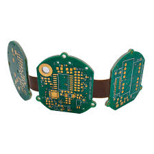
Can flexible PCBs be used in flexible displays?
To achieve this level of precision, flex PCBs must be made in layers, with the conductor width and spacing carefully calibrated to ensure they will bend without failing. This calibration process is called etching. For instance, a flex circuit’s conductor width should be no less than 0.375 millimeters. Conductor widths should also be evenly distributed across the board and avoid abrupt transitions from one trough to another.
The thickness of a flex PCB is also an important factor to consider. To improve its elasticity, manufacturers may choose to add what is known as a stiffener to selected areas. A stiffener is a rigid material (usually FR4) added to a flex PCB to increase its overall thickness. This increases the cost of the flex PCB, so it’s best to avoid these special requests if possible.
Other special requirements for flex PCBs include the use of a conductive adhesive or solder mask to protect the surface and reduce electrical interference. In addition, the PCB must be designed to have a minimum bend radius. This is a specific threshold below which the flex circuit will permanently deform or break.
Signal integrity is another crucial factor in flexible PCB design, especially as devices become more complex and operate at higher frequencies. The flexible nature of the PCB can introduce variability in the electrical performance, leading to issues like signal attenuation or crosstalk. To mitigate these risks, designers often employ techniques such as controlled impedance routing, differential pair design, and the use of ground planes. These strategies help maintain signal integrity by ensuring consistent electrical characteristics across the PCB, even as it flexes.
In the future, we can expect to see more innovative applications for flexible PCBs. Advanced technologies will allow manufacturers to build a range of products that are both functional and aesthetically pleasing. In particular, a leading smartphone manufacturer recently introduced a foldable phone that offers users a large dual-screen display while remaining compact when folded. Similarly, a popular fitness tracker uses flexible PCBs to offer a curved display that is optimized for the contour of a wearer’s wrist.