
HDI printed circuit boards
Printed circuit boards (PCBs) have evolved over time to support ever-shrinking devices. However, with increasing miniaturization comes the need to improve signal transmission, power management, and other functions in order to keep up with the technology. The industry has responded by implementing HDI PCBs which utilize microvias to increase wiring capacity while minimizing the space needed for the circuit board itself. Microvias are the smallest via holes on the market and they serve as pathways for electrical signals and power to travel between different layers of an HDI PCB. Microvias come in several forms, including stacked and staggered. The type of microvia chosen is based on the specific design and manufacturing process.
A microvia is a hole that has a diameter that is less than 150um (0.006 inches). According to IPC standards, a microvia must follow a 1:1 aspect ratio between its depth and its diameter. The most common types of microvias used in hdi printed circuit board are stacked and staggered. Stacked microvias are stacks of blind microvias that span between different layers. The buried microvias in the stack are then filled and plated, creating a connection between each layer. Staggered microvias are similar to stacked microvias, but the buried microvias in a staggered structure are offset from one another.
Both stacked and staggered microvias provide advantages over traditional through holes. Stacked microvias enable more components to be placed on a single surface and they can also reduce the overall thickness of the PCB. They are more efficient than through holes, enabling a smaller form factor and improving power delivery to the devices. They are also more reliable than through holes due to their small aspect ratio.
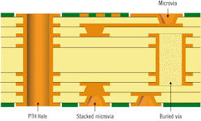
How are microvias used in HDI printed circuit boards?
However, despite the benefits of using microvias, they can be challenging to implement in the PCB manufacturing process. The extreme precision required for drilling them, combined with the complexity of their internal construction, can create reliability concerns. In addition, deviation from the optimal aspect ratio for a microvia can cause problems with the fill and plating processes.
The use of a laser drill for the creation of microvias helps to ensure accuracy and consistency in their geometry, which in turn enhances their performance. The copper foil material used for constructing them can have an impact on conductivity and heat dissipation, so designers need to strike the right balance between these factors. Additionally, proper signal tracing is critical to ensure that microvias work effectively in high-frequency applications.
This includes ensuring that the traces are wide enough and well-spaced to prevent signal loss and crossing delays. Achieving these objectives requires the right tools and processes to deliver the best results possible. The best option is to partner with a manufacturer that offers advanced capabilities and uses the latest technologies for PCB production. A reputable provider will employ HDI techniques such as laser drilling to maximize the potential of your PCB design and minimize risk throughout the assembly process.