
Importance of PCB Layout in Prototype Circuit Board Assembly
PCB circuit boards play a vital role in the manufacturing of modern electronic devices. They offer many advantages over traditional wired systems, such as fewer components, compactness and high reliability. However, they also come with several disadvantages, including high manufacturing costs and a lack of flexibility for fast iteration projects.
To overcome these shortcomings, engineers need to carefully design prototype circuit boards. This involves a series of critical steps, from requirements planning through the creation of CAD files for prototype fabrication.
The first step in prototype circuit board assembly design is to capture a schematic diagram of the project’s electrical connections. This is accomplished through the use of PCB design software, such as Eagle or KiCad. This process ensures that all components will fit on the board, and that traces will connect them properly. It is also important to understand the specifications of each component, and to compile a Bill of Materials (BOM) for all necessary supplies.
During this phase, it’s also necessary to determine the layer configuration of the prototype circuit board. This can be a single-layer, double-layer or multi-layer board, depending on the complexity of the project and space constraints. In addition, it’s critical to run a Design Rules Check, which helps to identify and correct potential problems before the final product is fabricated.
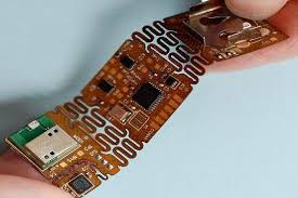
The Importance of PCB Layout in Prototype Circuit Board Assembly
After the layout of all components is determined, the next step is to apply solder paste to the surface of the PCB. Once the paste has been applied, the components are placed on their designated positions. To ensure accurate placement, engineers may utilize tools such as pick-and-place machines or reflow ovens. Once the components have been placed, they are soldered using either manual hot air soldering or a specialized process called wave soldering.
Finally, the finished product is inspected for any signs of damage or failure. It is also subjected to testing and reliability assessments to determine if it can withstand the environment and handling that it will be exposed to during operation. Typically, in the prototyping phase, the components used are not always the final ones. Designers often opt for readily available or simplified versions of the components to test the basic functionality of the circuit. Once the prototype has been tested and verified, the final design can be tweaked and improved as necessary before moving to full-scale production.
In the past, electronics were designed and assembled from a collection of small integrated circuits and discrete components connected by a multitude of wires. This method was inefficient, difficult to debug, and prone to mechanical failures. However, the development of the modern PCB circuit board revolutionized the way in which electronic products are designed and manufactured. Today, most electronics are built using PCB circuit boards.
To achieve this, a layered structure is used, with copper taking the place of wires to transmit electrical current. These circuits are then insulated by a non-conductive substrate, which protects the traces from external environmental factors. The final layers of the board include a solder mask, silkscreen and other components for protection and functionality.