
Thick Copper PCBs
Thick copper PCBs are used in a wide range of applications due to their superior current carrying capacity, thermal conductivity and resistance to corrosion. Their durability, robustness and high heat dissipation make them suitable for a variety of power electronics, automotive, aerospace and defence industry and medical equipment systems that need reliable operation under harsh environmental conditions.
In addition to their ability to handle higher current loads, thicker copper traces provide lower resistance, making them ideal for applications where minimizing voltage drops and power losses is crucial such as high-frequency RF circuits. Their enhanced heat dissipation properties also help prevent overheating, which can damage components and degrade performance.
The increased thickness of a thick copper pcb layer allows for the use of thinner dielectric materials between layers, which can reduce signal loss and improve transmission speed. However, using thin dielectrics can also increase the risk of electromagnetic interference (EMI). To mitigate this issue, a proper stack-up design is essential to achieve optimal performance and functionality.
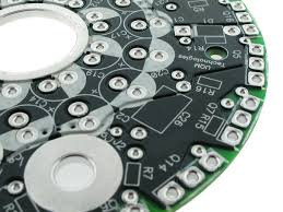
Thick Copper PCBs – Design Considerations
Choosing the right substrate for your PCB is another important factor to consider when designing thick copper PCBs. Depending on your application, you may need a standard FR-4 or other low-temperature material or an advanced substrate with higher glass transition temperature (Tg) to enable operation under extreme conditions.
PCBs with thicker copper layers require more careful manufacturing techniques and specialized equipment, which increases production costs. In addition, etching and laminating thicker copper can be more time-consuming, which can require multiple iterations to ensure the final product meets your design specifications.
Moreover, a thicker copper layer can lead to a larger area of conductivity and an increase in parasitic capacitance, which can increase your board’s overall impedance. As a result, you should carefully review your PCB’s current density and other electrical requirements to ensure that the final product is able to perform as expected.
If your design requires a higher voltage, there are several online tools you can use to determine what thickness, width or length your traces need to be in order to achieve your desired results. However, it’s best to consult with a PCB designer or expert to avoid over-designing and unnecessary expenses.
Moreover, the increased copper thickness enhances the mechanical strength and durability of the PCB, making it more resistant to mechanical stress, vibration, and bending. This makes thick copper PCBs suitable for harsh environments and applications subject to rough handling or extreme conditions.
Despite these benefits, manufacturing thick copper PCBs presents unique challenges compared to standard PCB fabrication processes. Specialized techniques such as sequential lamination and advanced plating methods are required to achieve the desired copper thickness uniformly across the PCB layers while maintaining tight tolerances and ensuring reliable electrical performance.
One other common concern when designing heavy copper PCBs is the need to balance the copper weight of each layer. It’s best practice to use the same copper weight on opposing layers, for example using 2oz on the outer layers and 1oz on the inner layers of a 4-layer PCB. This helps to ensure a balanced stack that reduces the risk of the board bending or twisting under operation.